Qualcomm QTM545: A Technical Deep Dive into 5G mmWave, Antenna-in-Package Design, and PCB Ground-Plane Reflection

Introduction
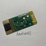
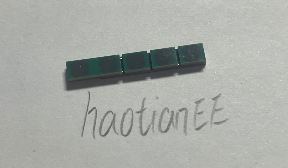
Recently, I have been investigating 5G millimeter-wave (mmWave) modules and came across a component marked QTM555. It belongs to Qualcomm’s QTM family, but publicly available documentation on this particular part appears to be scarce. Based on the package and its apparent application, one possibility is that it could be a customized variant related to the QTM545. However, without an official datasheet or confirmation from Qualcomm, this remains a hypothesis rather than an established fact.
This investigation led me down a broader technical rabbit hole: What makes mmWave 5G fundamentally different from conventional Sub-6 GHz systems? What exactly does 5G-Advanced mean? And perhaps most intriguingly, why can the same PCB ground plane that helps suppress electromagnetic interference also act as an electromagnetic reflector for a high-frequency antenna?
The last question is particularly interesting because it highlights a fundamental principle of RF engineering: the same physical structure can serve entirely different electromagnetic functions, depending on how it is excited and how the surrounding system is designed.
To understand why, let’s start with the basics of 5G and work our way down to the electromagnetic behavior of a ground plane.
1. Sub-6 GHz vs. 5G-Advanced: Understanding the Difference


Sub-6 GHz: The Practical Foundation of 5G
Most 5G deployments rely heavily on frequencies below 6 GHz, commonly referred to as Sub-6 GHz. These frequencies offer a practical balance between coverage, propagation characteristics, and available bandwidth.
Compared with mmWave, Sub-6 GHz signals generally experience less severe propagation loss over comparable distances and are better able to penetrate or diffract around certain obstacles. This makes them suitable for wide-area coverage, indoor connectivity, and everyday mobile communications.
In practical terms, Sub-6 GHz is the workhorse of 5G. It provides the coverage and reliability that most users expect from a cellular network.
Of course, actual performance depends on the frequency band, transmit power, antenna configuration, deployment density, and surrounding environment. A signal reaching an underground space, for example, depends heavily on the building structure and the availability of indoor coverage infrastructure.
mmWave: Trading Coverage for Bandwidth
Millimeter-wave communications operate at much higher frequencies, typically in the 24–100 GHz range under the broad engineering definition of mmWave. Commercial 5G deployments, however, use specific bands within that range, such as 26 GHz, 28 GHz, and 39 GHz, depending on the market.
The main attraction is bandwidth. Wider channel bandwidths make it possible to achieve extremely high data rates under favorable radio conditions.
In an ideal line-of-sight environment, with sufficient signal strength, suitable antenna arrays, and adequate network resources, mmWave can deliver peak data rates several times higher than those of typical Sub-6 GHz deployments.
But there is a trade-off.
At these frequencies, free-space path loss is higher for the same distance and antenna gains, and obstacles such as walls, human bodies, and even certain types of glass can significantly weaken the signal. mmWave systems therefore rely heavily on directional antennas, beamforming, and rapid beam management to maintain a usable connection.
In other words, mmWave is not simply a faster version of conventional 5G. It is a different engineering proposition: more bandwidth, more demanding RF design, and a greater dependence on antenna placement and propagation conditions.
Does 5G-Advanced Mean mmWave?
Not exactly. This distinction is worth making because the two terms are often used interchangeably in marketing discussions.
5G-Advanced, commonly marketed as 5.5G, is an evolution of the 5G system—not another name for mmWave.
3GPP Release 18 introduced the first set of 5G-Advanced capabilities, with further enhancements continuing in subsequent releases. These developments cover a broad range of technologies, including improvements to spectrum utilization, network efficiency, mobility, positioning, energy consumption, and support for advanced applications.
Both Sub-6 GHz and mmWave technologies can benefit from the broader 5G-Advanced ecosystem. The actual features available depend on the frequency band, network implementation, device capabilities, and operator deployment.
Therefore, deploying a mmWave module does not automatically make a system 5G-Advanced, just as operating a Sub-6 GHz network does not prevent it from supporting 5G-Advanced features.
The distinction matters when selecting hardware for industrial communications, robotics, remote operation, or other latency-sensitive applications. The radio module is only one component of a much larger system.
Latency: Why the Radio Link Is Only Part of the Story
Consider a remotely operated heavy truck traveling at 100 km/h.
At that speed, the vehicle moves approximately 27.8 meters per second. A communication delay of 50 milliseconds corresponds to a distance traveled of:
d=vt=27.8×0.05≈1.39 m
That is nearly 1.4 meters before accounting for braking-system response time or mechanical stopping distance.
This illustrates why latency matters in remote control. However, it is important to distinguish between radio-interface latency and end-to-end application latency.
A typical communication path may include:
- Radio transmission and reception over the air interface.
- Scheduling, retransmissions, and protocol processing.
- The radio access network, including the distributed unit (DU).
- Transport networks and core-network functions.
- User-plane routing, application processing, and the return path.
Under carefully engineered conditions, 5G systems can achieve very low radio-interface latency. Configurations using short transmission intervals, appropriate numerology, and mini-slot scheduling can reduce the time required to transmit a packet over the air.
In an optimized private network, the one-way radio-interface latency may reach the millisecond range or lower under suitable conditions. But that figure should not be confused with the total time required for a remote-control command to reach its destination and produce a response.
Retransmissions, beam switching, interference, congestion, processing overhead, and application design can all increase the delay.
For safety-critical applications such as remote driving or robotic surgery, low latency alone is not enough. The system also needs predictable performance, sufficient reliability, redundancy, and a well-defined fail-safe strategy.
This brings us to an important engineering principle: the fastest radio technology is not necessarily the best system unless the entire communication and control chain is designed around the application’s requirements.
2. PCB Ground Planes: From Noise Suppression to Electromagnetic Reflection


Let’s now look at the hardware itself.
A mmWave module such as a member of Qualcomm’s QTM family integrates RF circuitry and antenna structures into a compact package. Depending on the specific device, the antenna elements, RF front end, and associated interconnects may be integrated using an antenna-in-package (AiP) architecture.
In a simplified cross-sectional view, the structure may include antenna metallization, dielectric layers, RF interconnects, and one or more conductive ground planes.
At first glance, a large metal ground plane might seem to have a straightforward purpose: provide a low-impedance electrical reference, dissipate heat where the thermal design allows, and shield nearby circuitry.
Yet, when an antenna operates at mmWave frequencies, the same conductive structure can also play a crucial role in shaping the radiation pattern.
How can one piece of metal suppress unwanted electromagnetic effects in one situation while reflecting electromagnetic energy in another?
The answer lies in distinguishing conducted interference from radiated electromagnetic waves.
2.1 Why a Ground Plane Helps Suppress EMI
Digital circuits do not generate perfectly clean waveforms. Fast switching edges contain frequency components far beyond the fundamental clock frequency, and these components can excite unwanted currents and electromagnetic fields.
When current flows through a PCB trace, it must return to its source through a corresponding return path. If that path is poorly designed, the resulting current loop can become large, increasing inductance and making the circuit more susceptible to electromagnetic interference (EMI).
A well-designed ground plane helps by providing a continuous, low-impedance return path close to the signal trace.
This reduces the area enclosed by the signal and return-current paths, limits parasitic inductance, and helps control unwanted radiation.
For high-speed signals, the return current does not necessarily spread uniformly across the entire ground plane. At sufficiently high frequencies, it tends to concentrate in the region directly beneath the signal trace, where the electromagnetic field configuration favors the lowest-impedance return path.
This is why PCB layout engineers pay close attention to ground-plane continuity, reference-plane transitions, via placement, and return-current paths.
Adding ground vias can help connect ground regions and reduce the inductance of certain return paths, particularly when placed appropriately near high-frequency transitions. However, simply adding more vias does not guarantee better performance; their placement, geometry, and connection to the relevant reference planes matter.
It is common to hear that a ground plane “absorbs noise.” This is a useful introductory simplification, but it is not a complete physical description.
In most PCB designs, the primary mechanism is not that the ground plane absorbs every unwanted signal. Rather, it provides controlled current-return paths and helps contain electromagnetic fields. Some energy may be dissipated in conductive and dielectric losses, but much of the benefit comes from reducing the conditions that allow unwanted currents and fields to develop.
2.2 Why the Same Ground Plane Can Reflect mmWave Energy
Now consider the antenna.
When an antenna radiates, it establishes time-varying electric and magnetic fields. These fields extend into the surrounding dielectric and free space, carrying energy away from the RF source.
If a conductive ground plane is positioned near the antenna, the incident electromagnetic field interacts with the metal surface. The field induces surface currents, and those currents generate their own electromagnetic fields.
The resulting field is the combination of the incident field and the field produced by the induced currents.
Under suitable conditions, this interaction produces reflection and changes the distribution of electromagnetic energy around the antenna.
The ground plane is not simply absorbing the signal. Instead, it becomes part of the electromagnetic structure that determines how the antenna radiates.
This is a fundamental principle in antenna engineering. Conductive surfaces can provide shielding, define antenna boundaries, shape radiation patterns, and influence impedance matching.
The exact effect depends on the antenna geometry, the ground-plane dimensions, the separation between conductive layers, the dielectric properties of the package, and the operating frequency.
A ground plane placed at the wrong distance or designed with inappropriate dimensions can degrade antenna performance rather than improve it.
To understand the underlying mechanism, we need to look at the physics of electromagnetic reflection.
3. The Physics Behind the Mirror Effect


3.1 What Happens When an Electromagnetic Wave Reaches Metal?
Metals contain mobile charge carriers. When a time-varying electromagnetic field reaches a good conductor, it drives electric currents near the surface.
These induced currents generate additional electromagnetic fields. The boundary conditions at the metal surface constrain the combined fields, producing the familiar phenomenon of reflection.
For an ideal perfect electric conductor (PEC), the tangential component of the total electric field at the surface must be zero:
Et,incident+Et,reflected=0
This equation captures an important idea: at the conducting boundary, the incident and reflected tangential electric fields cancel.
The associated magnetic fields and surface currents must also satisfy the electromagnetic boundary conditions. The result depends on the orientation and polarization of the incident wave.
Real PCB ground planes are not perfect conductors, of course. Copper has finite conductivity, surface roughness, and frequency-dependent losses. Nevertheless, at many mmWave frequencies, a sufficiently thick, well-connected copper layer can behave approximately like a conducting reflector.
The important point is that the reflected field is not an unrelated copy of the original signal. It is a field generated through the electromagnetic response of the conducting boundary.
3.2 The Image Theory: An Antenna’s Electromagnetic Mirror
A particularly useful way to understand this behavior is through image theory, a standard technique in electromagnetics.
Imagine a simple antenna positioned above an ideal conducting plane.
Instead of solving the full field problem directly, image theory allows us to replace the conducting plane with an equivalent virtual source on the other side of the plane. The virtual source is positioned symmetrically and has an orientation and phase chosen to satisfy the boundary conditions.
This mathematical construction is called an image antenna.
It is not a physical antenna hidden inside the PCB. It is an equivalent source used to calculate the electromagnetic field in the region of interest.
The orientation of the image source depends on the original antenna’s orientation relative to the conducting surface. For example, a dipole oriented perpendicular to an ideal infinite PEC plane has an image current with the same direction, whereas a dipole parallel to the plane has an image current in the opposite direction.
This distinction is important because the popular explanation that a ground plane always creates an identical antenna with reversed current is not universally correct.
The image source must be derived from the actual geometry and electromagnetic boundary conditions.
In a real AiP package, the situation is more complicated than the idealized dipole-over-infinite-plane example. The antenna may consist of multiple elements, patterned metal layers, dielectric substrates, and integrated RF structures. Nevertheless, image theory provides a valuable starting point for understanding how nearby conductive layers affect radiation.
3.3 Why the Ground Plane Can Improve Antenna Performance
A properly designed ground plane can influence several important antenna characteristics.
Radiation direction. The ground plane can suppress radiation into certain directions and redirect more energy toward the intended side of the antenna.
Radiation efficiency. By limiting unwanted coupling into nearby structures and reducing certain forms of energy loss, the overall antenna system may achieve better efficiency. The actual result depends on the complete design.
Impedance matching. The ground plane changes the electromagnetic environment around the antenna, affecting its input impedance and resonance. Antenna geometry and matching networks must be designed accordingly.
Radiation pattern. The fields produced by the antenna and the induced currents on nearby conductors interfere with one another. Depending on their relative phases, this interference can reinforce radiation in some directions and reduce it in others.
However, a ground plane does not automatically improve every antenna parameter. An unsuitable size, position, or geometry can introduce unwanted resonances, detune the antenna, or distort the intended radiation pattern.
This is why mmWave antenna design relies heavily on electromagnetic simulation and measurement rather than intuition alone.
4. Antenna-in-Package (AiP): Making mmWave Integration Possible


At mmWave frequencies, antenna design becomes inseparable from package design.
Consider a signal operating at 28 GHz. Its free-space wavelength is approximately:
λ0=fc
Using the speed of light c≈3×10⁸ m/s:
λ0≈28×1093×108≈10.7 mm
That is a remarkably short wavelength.
In practical terms, a few millimeters of displacement, an unsuitable transition between layers, or an unexpected parasitic coupling path can significantly affect RF performance.
Inside a dielectric material, the wavelength becomes shorter still. In a simplified homogeneous, low-loss dielectric:
λd≈εrλ0
where εr is the relative permittivity of the material.
This is one reason why conventional PCB layout intuition cannot always be transferred directly to mmWave antenna design.
4.1 Why Put the Antenna Inside the Package?
Antenna-in-package technology integrates antenna structures into the semiconductor package rather than relying entirely on a separate, externally mounted antenna.
This architecture can offer several advantages:
- Shorter RF interconnects between the front end and antenna.
- Reduced interconnect losses compared with certain longer routing implementations.
- Compact integration of antenna arrays and RF circuitry.
- Better control over the relationship between antenna elements and package materials.
- Potentially easier integration of beamforming functions in compact devices.
AiP is particularly attractive for mmWave systems because the electrical length of interconnects becomes increasingly significant as frequency rises.
That said, AiP does not eliminate RF losses or layout challenges. Package materials, conductor roughness, antenna coupling, thermal behavior, manufacturing tolerances, and interactions with the host PCB still require careful engineering.
The package and the PCB should be treated as parts of one electromagnetic system.
4.2 Why Phased Arrays Matter
Many mmWave devices use multiple antenna elements rather than a single omnidirectional radiator.
By controlling the relative phases and amplitudes of the signals feeding these elements, the system can steer the main radiation beam in a desired direction. This technique is known as beamforming.
A simplified array model can be expressed as:
AF(θ)=n=0∑N−1anej(nkdsinθ+ϕn)
where:
- N is the number of antenna elements.
- an is the excitation amplitude of element n.
- d is the element spacing.
- k=2π/λ is the free-space or relevant propagation wavenumber.
- ϕn is the applied phase offset.
- θ is the observation angle under the chosen coordinate convention.
By adjusting the phase offsets, the array can reinforce radiation in a preferred direction and reduce it in others.
This is essential for mmWave communications because directional gain helps compensate for propagation losses and supports a usable link budget.
But beamforming also introduces new design requirements. Element spacing, mutual coupling, calibration, phase-shifter accuracy, packaging, thermal behavior, and the available scan angle all affect performance.
The ground plane remains part of this picture. It influences the electromagnetic environment of each antenna element and therefore affects the array’s behavior as a whole.
5. What Does This Mean for Qualcomm’s QTM545 and QTM555?
Returning to the original hardware investigation, it is tempting to infer a component’s capabilities from its package marking or resemblance to another device in the same product family.
That can be a useful starting point, but it is not sufficient evidence to identify the exact part.
A marking such as QTM555 may be associated with a specific product variant, a customer-specific configuration, an internal code, or another designation. Without an official datasheet, manufacturer confirmation, or a reliable traceable source, it would be premature to conclude that it is a customized version of QTM545.
For anyone investigating an undocumented mmWave module, I would recommend a few practical steps:
- Document the physical evidence. Record the package dimensions, visible markings, pin or pad arrangement, and any associated RF components.
- Look for authoritative documentation. Check manufacturer product pages, technical documents, regulatory filings, and module-level certification records where available.
- Inspect the surrounding design. Antenna placement, nearby RF components, board cutouts, shielding, and routing may help reveal the intended function.
- Avoid assumptions about pin compatibility. Similar package markings or dimensions do not guarantee identical electrical interfaces, RF performance, or firmware support.
- Validate through measurement. If the hardware can be safely powered and its interfaces are understood, RF measurements and controlled characterization can help establish its actual behavior.
These steps are particularly important for mmWave devices because package-level differences that appear minor visually can have substantial electrical consequences.
An undocumented part may look familiar while differing in antenna configuration, supported bands, RF front-end integration, calibration requirements, or host interface.
In RF engineering, visual similarity is a clue—not a specification.
6. Engineering Takeaways
The most interesting lesson from this investigation is not simply that a PCB ground plane can reflect electromagnetic waves. It is that electromagnetic behavior depends on the complete physical system, not on the name assigned to a piece of copper.
In digital design, a ground plane is often discussed in terms of reference potential, return-current continuity, and EMI control. In antenna engineering, that same conductive layer can become an essential part of the radiating structure.
There is no contradiction between these roles.
When dealing with conducted noise, a well-designed ground plane helps establish controlled return paths and reduce unwanted current loops. When dealing with a radiating antenna, the same plane interacts with electromagnetic fields, supports induced surface currents, and changes the resulting radiation pattern.
Both behaviors follow the same underlying electromagnetic laws.
The challenge is knowing which physical mechanisms dominate in a given structure—and designing accordingly.
For mmWave systems, that means paying attention to details that might seem negligible at lower frequencies: the dimensions of conductive features, dielectric properties, layer spacing, antenna orientation, package geometry, and the continuity of the reference plane.
It also means being careful with broad claims about 5G performance. mmWave can deliver exceptional data rates and support very low radio-interface latency under favorable conditions, but actual end-to-end performance depends on the entire network and application architecture.
Finally, when investigating hardware such as Qualcomm’s QTM545 or an undocumented component marked QTM555, the most reliable approach is to combine electromagnetic theory with traceable documentation and empirical validation.
That, to me, is what makes RF engineering fascinating: the same physical principles connect a seemingly ordinary sheet of copper on a PCB to antenna radiation, beamforming, interference control, and the behavior of an entire wireless communication system.