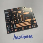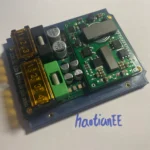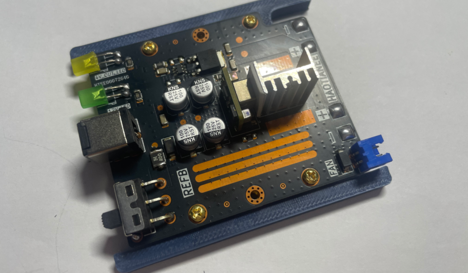

Quick Start Guide
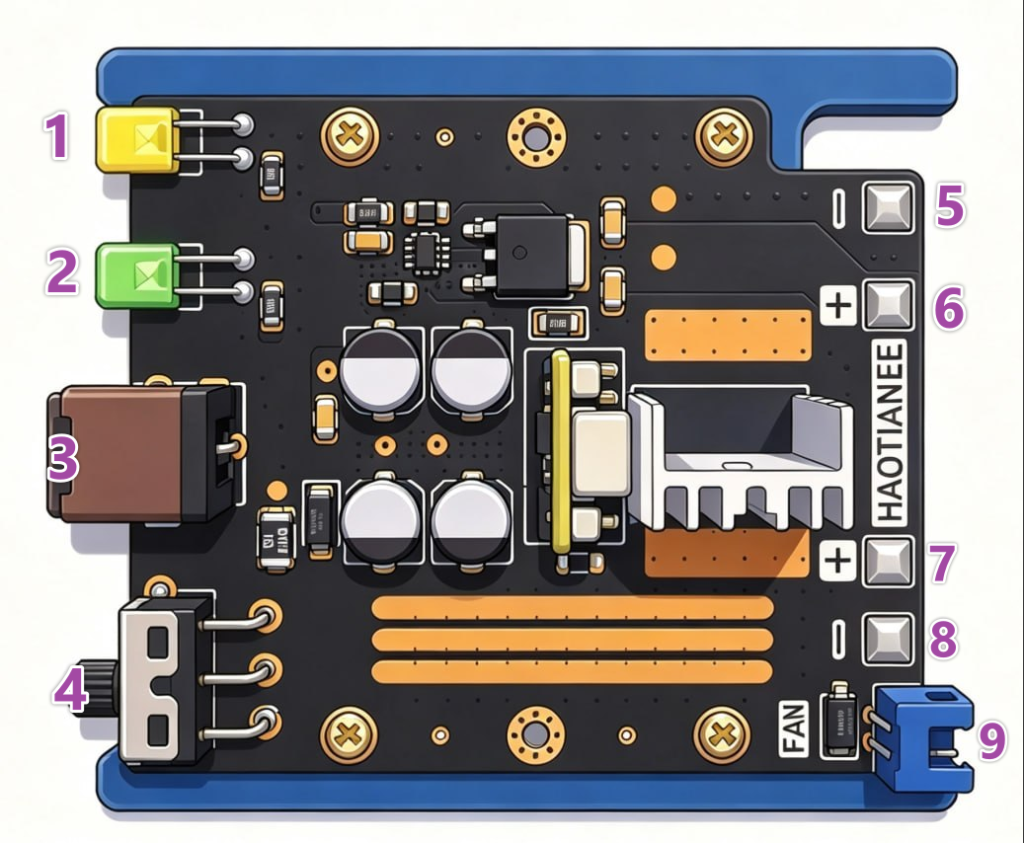
Board Interface Definitions
| No. | Interface / Indicator | Description |
|---|---|---|
| 1 | 4.15 V Output Indicator | LED indicator for the 4.15 V output. |
| 2 | 12 V Input Indicator | LED indicator for the 12 V input power. |
| 3 | DC 5521 Power Input (12 V) | DC 5.5 × 2.1 mm barrel jack for connecting a 12 V DC power adapter. |
| 4 | Main Power Switch | Main power switch for turning the board on or off. |
| 5 | 4.15 V Output (−) | Negative terminal of Output 1. |
| 6 | 4.15 V Output (+) | Positive terminal of Output 1. |
| 7 | 4.15 V Output (−) | Negative terminal of Output 2. |
| 8 | 4.15 V Output (+) | Positive terminal of Output 2. |
| 9 | XH2.54 Fan Connector (12 V) | 2.54 mm-pitch XH-series connector providing 12 V for an external cooling fan. Based on the connector orientation shown in the image, the upper pin is negative (−) and the lower pin is positive (+). Verify the polarity before connecting a fan. |
Important Notes
- Use a 12 V DC power adapter with a 5.5 × 2.1 mm (5521) barrel plug for the DC input.
- Verify the output polarity before connecting the board to a smartphone.
- For the fan connector, confirm the pin orientation against the actual board before applying power. The upper-negative, lower-positive arrangement is based on the image orientation and should be verified on the physical board.
Board Details
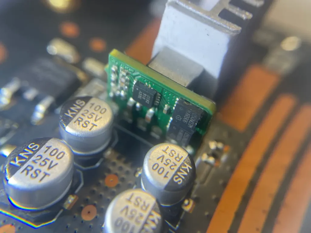
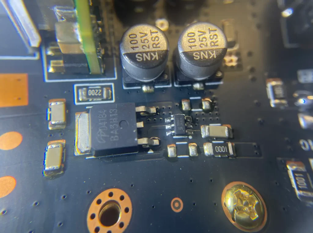
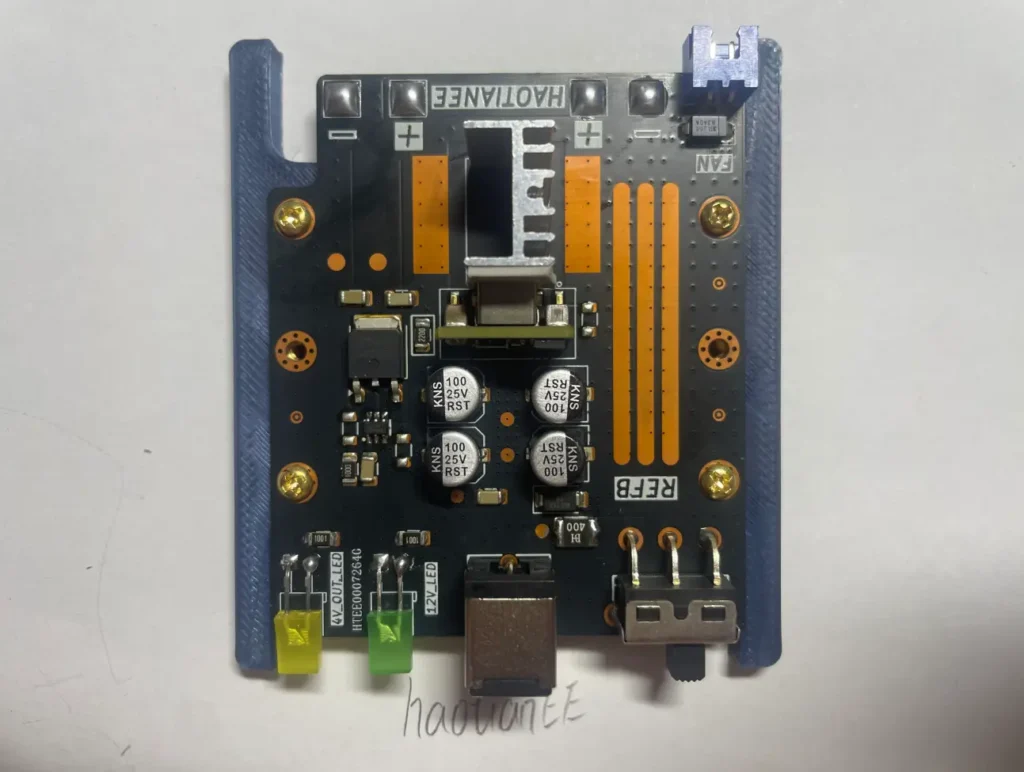
- Quick Start Guide
- 1. Overview
- 2. System Architecture
- 3. Key Design Features
- 4. Hardware Specifications
- 5. Connector Identification and Wiring
- 6. First-Time Setup and Operating Procedure
- 7. Electrical Safety and Compatibility
- 8. Troubleshooting
- 9. Technical Validation and Performance Reporting
- 10. Design Summary
1. Overview
1.1 Purpose
The TPS40192 Smartphone Battery Bypass Power Supply Board is a custom DC power module designed to supply a smartphone’s battery power input from an external 12 V DC source.
It converts the 12 V input into a regulated 4.15 V output, allowing compatible smartphone hardware to operate without relying on its original rechargeable battery. The design is intended for applications such as motherboard testing, firmware development, device refurbishment, long-duration testing, and unattended operation.
Many smartphones are not designed to operate with the battery physically removed. Depending on the model, the device may monitor battery voltage, temperature, identification, or communication signals before allowing normal startup. Consequently, connecting a conventional USB power supply to a phone with its battery removed may not be sufficient.
A dedicated battery bypass supply addresses the power-delivery part of this problem by providing a low-voltage, high-current source at the battery power input.
Important: Supplying the correct battery voltage does not guarantee that every smartphone will boot without its battery. Battery temperature sensing, identification pins, battery-management electronics, and model-specific startup requirements may still need to be addressed separately.
1.2 Why use an external battery bypass supply?
Rechargeable batteries can be inconvenient in devices that must operate continuously for extended periods. Keeping a battery permanently connected to a charger or at a high state of charge may accelerate degradation under some conditions. Aging batteries can also develop increased internal resistance, causing voltage drops during high-current operation.
For a phone used as a test platform, automation device, or development target, replacing the battery’s power-delivery function with a properly designed external supply can simplify maintenance and make power conditions easier to control.
This board was developed for a specific practical requirement: the phone must run for long periods under potentially high loads, while its USB-C port remains available for peripherals, debugging, or other connections.
The board provides a dedicated battery-side power path rather than relying on the phone’s USB-C charging input.
1.3 Intended applications
- Smartphone motherboard testing and repair.
- Firmware flashing and software development.
- Long-duration stability and unattended-operation testing.
- Automated smartphone test stations.
- Battery-free operation of compatible phone hardware.
- Power delivery to compatible devices requiring a nominal 4.15 V supply.
The board is intended for engineering and laboratory use. Compatibility must be confirmed for each device model before operation.
2. System Architecture
12 V DC Input
Regulated external DC supply
Synchronous Buck Converter
TPS40192 controller and external power stage
4.15 V Regulated Output
High-current battery-side supply
MOSFET-Based Ideal-Diode Stage
MX5050T controller and external MOSFET, as described by the design
Smartphone Battery Power Input
Connect using the correct model-specific battery interface
Figure 2. Functional block diagram based on the supplied project description. Confirm the actual circuit connections and protection behavior against the board schematic.
The power path consists of two main stages.
Stage 1 — Voltage conversion: The TPS40192 controls a synchronous buck power stage that steps the 12 V input down to a nominal 4.15 V output.
Stage 2 — Reverse-current protection: An ideal-diode circuit based on the MX5050T and an external MOSFET is intended to reduce forward voltage loss and prevent reverse current through the protected power path.
The TPS40192 is a controller rather than a complete integrated buck converter. The external MOSFETs, inductor, capacitors, feedback network, and PCB layout are essential parts of the power stage. The board’s actual current capability therefore depends on the complete implementation, not on the controller specification alone.
3. Key Design Features
3.1 Fixed 4.15 V Output
The board is configured for a nominal output voltage of 4.15 V.
This voltage is close to the fully charged voltage used by many single-cell lithium-ion battery systems. However, smartphone battery interfaces and power-management designs vary, and 4.15 V should not be treated as a universal battery voltage for all phones.
The fixed-voltage design avoids the need to adjust an output voltage for every normal startup. It also reduces the chance of accidental adjustment to an unsuitable setting during routine laboratory use.
Before connecting a phone, verify the output voltage with a multimeter. For precision work, also check the voltage at the actual load connection under load, because cable and contact resistance can produce voltage differences between the board and the phone.
Output current and power
The design description states that the power stage has a theoretical output capability of up to 10 A and recommends limiting continuous operation to 5 A or less.
At 4.15 V, these figures correspond to the following nominal output power:
| Output current | Nominal output power |
|---|---|
| 1 A | 4.15 W |
| 3 A | 12.45 W |
| 5 A | 20.75 W |
| 10 A | 41.5 W |
These are calculated electrical values, not measured efficiency or thermal-performance results.
The 10 A figure should be understood as a theoretical design capability unless supported by documented load testing. The recommended 5 A continuous operating limit is the more conservative starting point, but it should not be considered a guaranteed safe rating until the board’s temperature rise, wiring, connectors, and protection behavior have been verified under representative conditions.
3.2 Ideal-Diode Reverse-Current Protection
The board uses a MOSFET-based ideal-diode arrangement described as combining an MX5050T controller with an external MOSFET.
A conventional Schottky diode introduces a forward-voltage drop and associated power loss. An ideal-diode circuit uses active MOSFET control to reduce this loss while managing current direction.
The intended benefits include:
- Lower forward voltage drop than a conventional diode in suitable operating conditions.
- Reduced conduction losses and heat generation.
- Blocking reverse current when the circuit operates within its specified conditions.
- Additional isolation between the output and the upstream power path.
The author also describes protection against reverse current associated with external USB-C PD charging.
That behavior should be verified against the complete schematic before relying on it. The presence of an ideal-diode stage in one power path does not automatically protect every connection on the board, nor does it guarantee protection against every possible external power source or transient.
Do not connect a USB-C PD charger and the bypass supply simultaneously until the relevant current paths have been confirmed from the schematic and tested.
3.3 PCB Layout and Thermal Management
High-current DC power design depends heavily on PCB layout and thermal performance.
The board uses short power-current paths, broad copper areas in high-current regions, and a heatsink associated with the inductor, according to the project description.
These features are intended to reduce conduction losses and manage heat during prolonged operation.
Several factors remain important during real-world use:
- Inductor temperature under continuous load.
- MOSFET conduction and switching losses.
- Input and output capacitor ripple-current ratings.
- Connector and solder-joint temperature.
- PCB copper thickness and effective current-carrying area.
- Cooling airflow and ambient temperature.
- Voltage drop across the external wiring.
A heatsink can help dissipate heat, but its presence alone does not establish a safe operating temperature. Actual thermal performance should be checked after the board has reached steady-state operation under load.
4. Hardware Specifications
The following table separates the design information supplied by the author from details that still require verification.
| Parameter | Specification |
|---|---|
| Main controller | TPS40192 |
| Conversion topology | Synchronous buck |
| Nominal input voltage | 12 V DC |
| Controller operating input range | 4.5–18 V, according to the IC datasheet |
| Nominal output voltage | 4.15 V |
| Theoretical output-current capability | Up to 10 A, as stated by the author; not independently verified |
| Recommended continuous output current | 5 A or less, as stated by the author |
| Reverse-current protection | MX5050T-based ideal-diode stage, according to the design description |
| Output arrangement | Two output paths are described; exact pinout and electrical relationship require confirmation |
| Cooling provision | Inductor heatsink; 12 V fan connection provided |
| Intended use | Smartphone battery bypass, motherboard testing, firmware work, and long-duration operation |
The TPS40192’s own 4.5–18 V input range is an IC specification. It does not establish that every voltage within that range is a validated operating condition for this particular board. The recommended external input remains 12 V DC unless the board designer documents otherwise.
The following items should be added to the final hardware specification after verification:
- Permitted input-voltage tolerance.
- Maximum input current.
- Output-voltage tolerance and ripple.
- Continuous and peak output-current limits.
- Overcurrent and short-circuit behavior.
- Reverse-current test conditions.
- Operating ambient-temperature range.
- Exact connector types and pin assignments.
5. Connector Identification and Wiring
This section is intended to serve as the practical wiring reference for the board.
The exact connector pinout must be confirmed from the PCB silkscreen or schematic before power is applied. The supplied photograph is not clear enough to establish every connector’s polarity or pin numbering reliably. The labels below describe the required electrical functions, not verified physical pin positions.
5.1 DC Input: 12 V
The input supplies the energy required by the buck converter and its downstream load.
| Signal | Function | Connection |
|---|---|---|
| VIN+ | Positive DC input | Connect to the positive terminal of a regulated 12 V supply |
| VIN− / GND | DC input return | Connect to the negative terminal of the supply |
Use a regulated 12 V DC source with sufficient current capacity for the expected output load. Confirm the board’s actual input connector and polarity before connecting the supply.
Do not assume that an arbitrary connector terminal is VIN+ merely because of its physical position. Use the PCB markings and schematic to identify the correct terminals.
5.2 Smartphone Power Output
The board description specifies two output paths intended to accommodate certain dual-cell or foldable smartphone configurations.
However, the electrical relationship between these outputs must be confirmed before use. Two connectors do not necessarily mean two independent, isolated power supplies, and they must not automatically be connected in parallel or series.
| Signal | Function | Required action |
|---|---|---|
| OUT+ | Positive battery-side supply | Connect to the verified positive battery terminal |
| OUT− / GND | Power return | Connect to the verified battery negative terminal |
| Output 1 | First documented output path | Verify its terminal mapping and supported load |
| Output 2 | Second documented output path | Verify its terminal mapping and supported load |
Before connecting the output to a phone, identify the battery connector’s positive and negative terminals from the device’s service documentation or the original battery’s markings.
Do not infer battery pin assignments from wire color alone.
Some smartphones use additional battery terminals for a temperature sensor, battery identification, or battery-management communication. The 4.15 V supply does not automatically reproduce these signals. If a phone requires them for startup, the appropriate model-specific solution must be implemented separately.
5.3 Optional 12 V Cooling Fan
The board description mentions a 12 V fan connection.
Before installing a fan, verify the connector’s polarity, voltage rating, pin count, and whether it provides a continuously powered output or a controlled fan signal.
| Signal | Function |
|---|---|
| +12 V | Fan supply, if confirmed by the PCB marking |
| GND | Fan return, if confirmed by the PCB marking |
Do not connect a 5 V or 3.3 V fan to a confirmed 12 V supply. Likewise, do not assume that the fan header is protected against reverse polarity or excessive current.
5.4 Wiring Overview
12 V regulated DC supply
Positive to verified VIN+, negative to verified VIN−.
TPS40192 power board
Steps the input down to the nominal 4.15 V output.
Compatible smartphone
Connect the verified battery positive and negative terminals. Address additional battery-sensing requirements separately.
Figure 3. Functional wiring overview, not a physical connector pinout. Confirm all terminals on the actual board before wiring.
6. First-Time Setup and Operating Procedure
Follow this sequence when using the board for the first time or connecting it to a new smartphone model.
Step 1 — Inspect the hardware
Check the PCB for damaged components, solder bridges, loose connectors, or signs of overheating. Confirm that the input connector, output connector, and fan header match the board documentation.
Step 2 — Connect the 12 V input
With the supply switched off, connect its positive and negative leads to the verified input terminals. Set the source to 12 V and use an appropriate current limit for the initial test.
Step 3 — Verify the output voltage
Power the board without a smartphone attached. Measure the output at the intended connection points and confirm that the polarity is correct and the voltage is approximately 4.15 V.
Step 4 — Check the phone’s battery interface
Confirm the battery connector pinout, polarity, and any additional temperature-sensing or identification requirements. Do not connect the power output until the interface has been positively identified.
Step 5 — Connect and test under load
Switch off the power before making the connection unless the board’s documentation explicitly permits hot-plugging. Start with a low-load test, observe startup behavior, and increase the load gradually while monitoring voltage, current, and temperature.
The images above are illustrative references for the test procedure, not photographs of the actual XhtCore-style power board or verified demonstrations of its performance.
Recommended Initial Test Conditions
For a new board or an unfamiliar phone, begin with a conservative test rather than immediately applying the maximum rated load.
- Verify the output voltage and polarity before attaching the phone.
- Use a current-limited bench supply for initial testing.
- Keep the recommended continuous output limit of 5 A or less unless further test data establishes another limit.
- Monitor the regulator, inductor, MOSFETs, connectors, and wiring for abnormal heating.
- Record the phone model, test duration, observed current, and any startup or stability issues.
- Stop testing immediately if the output becomes unstable, a component overheats, or there is evidence of reverse current or a wiring fault.
The appropriate current limit depends on the phone and the power board. A bench supply’s current-limit setting should not be treated as a substitute for verified board-level overcurrent protection.
7. Electrical Safety and Compatibility
A battery bypass supply replaces the battery’s electrical power source; it does not necessarily replace every function of the original battery pack.
7.1 Battery-Sensing Requirements
A smartphone may require a valid battery-temperature signal, identification resistor, battery-management interface, or other model-specific signal before it will boot or operate normally.
If the phone does not start despite a correct 4.15 V supply, check its battery-interface requirements rather than increasing the output voltage arbitrarily.
Never assume that a phone’s battery connector contains only positive and negative terminals.
7.2 Reverse Current and USB-C PD
The ideal-diode circuit is intended to manage reverse current in its protected path. Nevertheless, USB-C power delivery and battery bypass wiring can create multiple possible current paths.
Do not connect the board to a phone while simultaneously introducing another source of power through USB-C until the circuit has been verified to prevent unintended source-to-source current flow.
A USB-C PD port must not be assumed to be reverse-current protected merely because the battery-side output includes an ideal-diode circuit.
7.3 Short Circuits and High Current
At 4.15 V and 5 A, the output can deliver approximately 20.75 W. Even though the voltage is low, a short circuit can produce high current, intense local heating, damaged connectors, or PCB damage.
Use properly rated wires and connectors, avoid exposed conductive surfaces, and disconnect the supply before changing wiring. Verify the board’s short-circuit response rather than assuming that the controller’s protection features guarantee protection for the entire assembly.
7.4 Thermal Management
The board includes a heatsink for the inductor and a provision for a 12 V fan.
If the board will be operated continuously, thermal performance should be evaluated at the intended ambient temperature and load. A fan may improve cooling, but it does not compensate for undersized conductors, poor connections, inadequate component ratings, or an incorrectly configured power stage.
8. Troubleshooting
| Symptom | Possible cause | Recommended checks |
|---|---|---|
| No output voltage | Input polarity error, missing input power, or converter fault | Verify the 12 V input, wiring, and power-stage components |
| Output is not 4.15 V | Incorrect feedback configuration, overload, or circuit fault | Measure the output without a load, then test with a controlled load |
| Phone does not boot | Incorrect battery pinout or missing battery-sensing signals | Confirm the phone’s battery-interface requirements |
| Phone restarts under load | Voltage drop, transient response, excessive current, or poor connections | Measure voltage at the phone connector during startup and load changes |
| Excessive component temperature | High losses, poor cooling, overloaded output, or bad connections | Reduce the load and inspect thermal behavior |
| Unexpected current from another port | An unintended reverse-current path or simultaneous power sources | Disconnect external sources and review the circuit’s current paths |
| Fan does not run | Incorrect fan rating, polarity, or header configuration | Check the fan connector markings and measure its supply |
Troubleshooting should proceed from basic electrical checks to more detailed circuit analysis. Do not increase the output voltage to compensate for a voltage drop until the cause has been identified.
9. Technical Validation and Performance Reporting
For a technical document intended to support engineering use, measured results are more valuable than broad claims about stability or maximum output current.
The following tests are recommended before publishing a final, validated specification.
| Test | What to record |
|---|---|
| No-load output | Output voltage and input current |
| Load regulation | Output voltage at several documented current levels |
| Output ripple | Peak-to-peak ripple, measurement bandwidth, probe method, and load |
| Load transient | Voltage response to a documented load step |
| Thermal soak | Component temperatures after a defined period at a specified load |
| Reverse-current protection | Test setup, current direction, and measured behavior |
| Short-circuit response | Protection behavior and recovery procedure |
| Continuous operation | Load, ambient temperature, test duration, and any faults |
These tests should be performed with suitable instruments and documented test conditions. Until results are available, the 10 A theoretical capability and the recommended 5 A continuous limit should remain clearly distinguished from independently verified performance.
For component-level reference, consult the official Texas Instruments TPS40192 datasheet and the MX5050T datasheet . Component specifications should not be substituted for validation of the assembled board.
10. Design Summary
The TPS40192 Smartphone Battery Bypass Power Supply Board is designed to provide a nominal 4.15 V, high-current supply from a 12 V DC source for compatible smartphone battery interfaces.
Its main design features include a synchronous buck power stage, a MOSFET-based ideal-diode circuit, broad copper power paths, inductor cooling, and two described output paths for certain applications.
For engineers and technicians, the most important considerations are not only the nominal voltage and current figures, but also connector polarity, phone-specific battery sensing, reverse-current behavior, cable resistance, and thermal performance.
The board can be useful for motherboard debugging, firmware testing, and long-duration operation when the target phone’s requirements are understood and the electrical interface is connected correctly.
The final operating limits should be based on measured performance and documented test conditions rather than theoretical component capability alone.